

We have a professional PCB processing, can provide you with professional PCB board size batch processing operations, and rapid PCB prototype proofing urgent, professional production of high-density, high-precision single-sided, double-sided and multilayer rigid PCB board and soft PCB board. Production levels up to 32 layers, the minimum line width from 3mil, the smallest laser aperture 4mil, the smallest mechanical aperture 8mil, and buried with blind hole hole production. PCB board to meet your various requirements, such as lead-free ROHS environmental protection requirements, Gold Finger, Immersion Gold and other process requirements. Through the introduction of Germany, Japan, Hong Kong, Taiwan and other countries and regions with advanced PCB production, processing, testing equipment, and constantly improve production efficiency and economic efficiency.Product range:Currently processed products have been widely used in computers, telecommunications, network, household appliances, instrumentation, medical, industrial, automotive, semiconductors, microelectronics, LCD and LED, mobile phone camera modules and other fields.Technical support:Dedicated to domestic and foreign enterprises, factories, traders, research institutes to provide complete production services board and a strong technical support.Workshop:R & D process, stability and support customer projects and production schedules, capture the market opportunities.Process Capability:Maximum number of layers: 32 layersMinimum line width spacing: 3milMinimum laser aperture: 4milMinimum mechanical aperture: 8milCopper foil thickness :18-175 §èm (standard: 18§èm35§èm70§èm)Peel strength: 1.25N/mmMinimum punching aperture: Single: 0.9mm/35milMinimum hole diameter: 0.25mm/10milAperture tolerance: ¡Ü ¦Õ0.8mm ¡À 0.05mmHole tolerance: ¡À 0.05mmHole wall copper thickness: double / multi-layer: ¡Ý 2um/0.8milHole resistance: double / multi: ¡Ü 300§è¦¸Minimum line width: 0.127mm/5milMinimum distance: 0.127mm/5milSurface treatment: spray tin rosin electric gold, anti-oxidation, of gold, carbon oilWarp: ¡Ü 0.7%ROHS lead-free requirements of environmental protection can be achieved, Gold Finger, Immersion Gold and other technical requirementsTwo-panel 24-hour fast processing can be completed in 4 to 8 layers processing cycle can be 48-72 hours of delivery
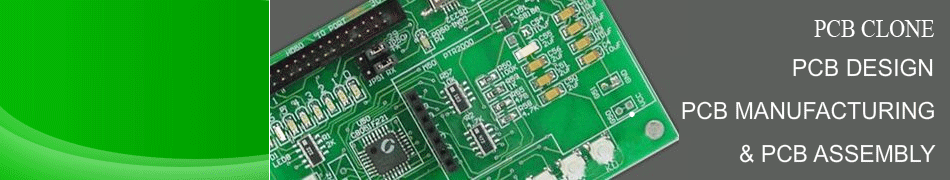
???We processed products are epoxy glass fiber material FR4, CEM1, CEM3, BT material, thick copper circuit boards, high TG circuit boards, aluminum heat board, ultra-thin ultra-small thick gold circuit board, mobile phone battery button board Halogen-free board, Rogers High frequency board, backplane and other high-level numbers. Product process, including spraying of pure tin, gold, Immersion Gold, Immersion Silver, Immersion Tin, OSP (anti-oxidation board), high TG, aluminum panels.
???Hetell team through the company’s unremitting efforts, has successfully developed the mechanical micro-hole, high aperture ratio, high number of backplane, high-precision impedance, HDI and other leading production technology, can provide you with PCB production process ¹ý³Ì was resolved programs can also be tailored to your model.
???Current delivery capacity of the factory on printed circuit boards up to 1200 square meters, the sample pairs of panels can be finished in 24 hours, 4-8 layers up to 3-5 day processing period, volume two-panel 3-5 days, 4 to 8 layers 5-8 days.